
Overview
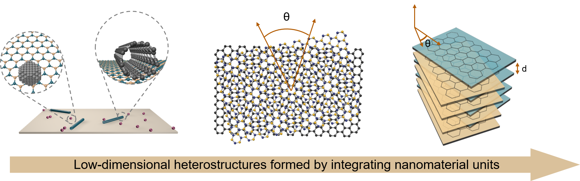
The research in our group focuses on the bottom-up assembly of micro-, meso-, macro-scale materials from nanomaterial units, the discovery of their unique optical, electrical, mechanical, and chemical properties, and the development of their functionalities. Our research includes: (1) Fabrication of low-dimensional heterostructures and crystals; (2) Optical spectroscopy and microscopic imaging at the interfaces; (3) Development of functionalities and optoelectronic devices. |
Just like organic chemists who use atoms to build molecules with different structures and activities, after assembling different atomically-thin 2D material units layer-by-layer, people will get artificial superlattices and crystals with fully unexplored properties and functionalities. Benefiting from the great success of the structure-property relationship study on single nanomaterial units, our main research interests include physical/chemical strategies towards the fabrication of low-dimensional heterostructures, superlattice and crystals. In collaboration with material synthesis groups, we aim to build atomic-level precision novel structures and materials from components, micro-scale structures, interfacial distance and twist angles. Micro-nano fabrication technologies, physical/chemical vapor deposition technologies, aligned transfer and origami techniques, interfacial and confined chemical reactions are representative tactics we will employ. |
 |
Selected Publications |
|
Nanomaterial unit exhibits remarkable surface and interface effect. Electron motions at the interface usually determine the overall property of a low-dimensional heterostructure. For example, graphene and monolayer transitional metal dichloride (TMD), carriers at the interface are under an atomic-level steep potential field gradient, which provides an excellent platform for the study of quantum tunneling and other low-dimensional interface carrier dynamics. Our research focuses on the nano-scale interface interactions in low-dimensional heterojunctions with different coupling states, using spatio-temporal resolved spectroscopy, dynamically correlated real-space and momentum-space multi-field optical imaging technology, as well as surface-enhanced spectroscopic technologies, to discover novel physical and chemical phenomena at interfaces from different coupling structures. Besides the in-depth understanding of nano-scale interfacial interaction laws, we will use various external fields such as light, electric field, temperature and pressure, to develop strategies towards nano-scale interface carrier engineering and to provide ideas for the design and development of new optoelectronic devices. |
 |
Selected Publications |
|
Through the reassembly of single-layer or multilayer materials such as graphene (semi-metal), boron nitride (insulator) and molybdenum disulfide (semiconductors) obtained by decoupling a series of van der Waals crystals, people have explored application scenarios such as light-emitting diodes, interlayer excitons and moiré excitons, interface superconductivity, anisotropic thermal materials, etc. Towards the development of functional materials and optoelectronic devices, our research group will use basic units such as small molecules, nano-carbon materials, transition metal dichalcogenides, boron nitride, plasmon metals and perovskite materials, focusing on functionalities and devices closely related to interface coupling effects, including exciton emission, artificial chiral structures, acoustic sensing, nonlinear optics, and optoelectronic logic devices. We will strive to achieve breakthroughs from basic scientific research to industrial applications. |
 |
Selected Publications |
|

